


Toshiba Electronics Europe has introduced five new automotive MOSFETs designed to support compact, high-reliability power electronics in vehicle systems, including electric vehicles (EVs).
The lineup includes four N-channel (XSM6K361NW, XSM6K519NW, XSM6K376NW, and XSM6K336NW) and P-channel (XSM6J372NW) devices, all housed in the DFN2020B(WF) package with a wettable flank structure.
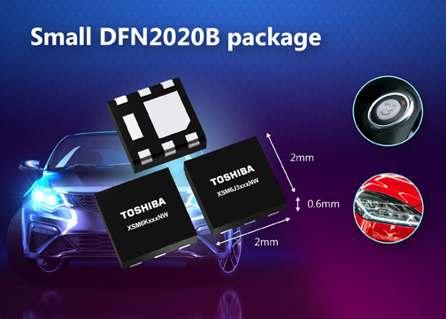 The DFN2020B(WF) package is designed to improve solder joint inspection and mechanical reliability.
The wettable flank structure enhances solder wettability and allows solder fillet visibility for Automated Optical Inspection (AOI), supporting quality control in automotive manufacturing. In shear strength testing, the package demonstrates approximately 23% higher strength compared to Toshiba’s SOT-23F package.
With a typical size of 2.0 × 2.0 × 0.6 mm, the DFN2020B(WF) package reduces mounting area by approximately 43% and height by approximately 25% compared to SOT-23F. This supports continued miniaturization in vehicle electronics, including space-constrained EV subsystems.
Despite the smaller footprint, the devices maintain high power dissipation capability. For example, the XSM6K361NW is rated for 1.84 W, approximately 1.5 times higher than comparable devices in the SOT-23F package. This enables use in applications such as dc-dc converters for ECUs and load switching, which are also relevant to EV power distribution and auxiliary systems.
The MOSFETs meet AEC-Q101 reliability standards, and PPAP documentation aligned with IATF16949 is available, supporting integration into automotive and EV production environments.
Toshiba plans to expand its MOSFET portfolio using the DFN2020B(WF) package, including future 2-in-1 configurations for automotive applications.
Filed Under: Power Electronics, Technology News